| Achieved Fmax | 160 MHz |
|---|---|
| Constraint Met | 100 MHz with +3.759 ns slack |
| Peak Throughput | 6.4 GMACs/sec at 100 MHz |
| DSP48E1 | 64 / 240 (26.67%) |
| LUTs | 1,562 / 63,400 (2.46%) |
| Flip-Flops | 4,193 / 126,800 (3.31%) |
| Latches | 0 |
| Verification | 10,000 / 10,000 random matmuls bit-exact vs NumPy |
I started this looking at where transformer inference actually spends its cycles. On a CPU, the answer is what you’d guess: matrix multiplication takes most of the wall clock, and inside the matmul most of the time is waiting on memory rather than doing arithmetic. CPUs can run multiplies faster than they can fetch operands, which is most of why GPUs and dedicated accelerators exist in the first place.
A systolic array is one of the cleaner ways around that. The idea isn’t new (Kung and Leiserson, 1978), but it’s the same architecture sitting at the core of Google’s TPU today. You build a grid of multiply-accumulate cells, stream operands through it, and each operand gets reused across many cells before it leaves. One memory read buys many compute operations.
This project is my implementation of that idea at 8×8, verified at the level I’d want to see if someone else were handing it to me. It’s the first of seven milestones in my undergrad capstone, building toward a compute-in-memory transformer accelerator on FPGA.
Architecture
The design has three pieces. A skew unit staggers the inputs in time. An 8×8 grid of MAC cells does the actual work. A controller keeps track of when the answer is ready.
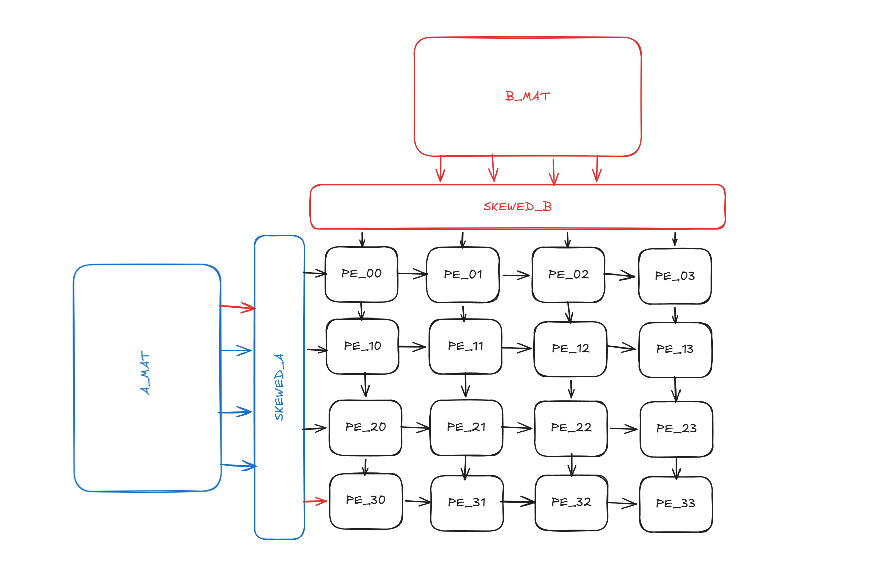
Fig. 1 — Block diagram. The skew unit transforms two parallel input matrices into the diagonally-staggered streams that feed the PE mesh’s west and north edges.
The Processing Element
Each cell does one multiply and one add per clock cycle, holds the running sum in a register, and forwards its inputs east and south. The dataflow is output-stationary, meaning the partial sum stays put while the operands flow through. That’s the right choice when you compute each output once and read it once. Adding a write-back path for partial sums would just be wasted hardware.
The accumulator is INT32 even though both inputs are INT8. That’s headroom, not laziness. The largest possible single product is 128 × 128 = 16,384, and you can fit 256 of those before you risk overflowing INT32. For an 8×8 array doing K=8 accumulations per output, that’s 8× more headroom than I actually need, but INT32 is the natural width on this DSP, and anything narrower would just bring in saturation logic.
I tagged the multiply with the (* use_dsp = "yes" *) synthesis attribute. Without it, Vivado will sometimes decide to use LUTs for an 8×8 multiply instead of a dedicated DSP slice, and the resulting design loses about 40 MHz of headroom. With the attribute, every PE maps to exactly one DSP48E1.
The Skew Unit
This was the part that took me the longest to get right.
A systolic array needs its inputs to arrive in a staggered diagonal pattern. The top-left PE needs A[0][0] and B[0][0] on the first cycle. The cells one step diagonally need A[0][1]/A[1][0] and B[0][1]/B[1][0] one cycle later, and so on. If you feed the array the matrices as they’re laid out in memory, the answer comes out wrong because partial sums from different rows mix together.
There are two common ways to implement that stagger. One is to use shift registers, physically delaying each row by a different number of cycles by chaining flops. It works, but it spends flops you don’t really need. The other way is the one I went with: keep the matrices in registers and use a counter to read the right element on the right cycle. Row r is valid for K cycles starting at cycle r. Column c is valid for K cycles starting at cycle c. The counter approach uses fewer registers and the hardware is essentially free, since it’s just an indexed read into a small array.
There’s one subtle thing about the timing of the start signal that’s worth mentioning. The signal that says “we’re skewing now” is set in one always_ff block, and it’s read in a different always_ff block. Because of how non-blocking assignments work in SystemVerilog, the second block sees the old value of the signal during the cycle when the first block updates it. So the first skewed element comes out one cycle after start is pulsed, not on the same cycle. That happens to be exactly the one-cycle pipeline-fill delay the PE mesh expects, so the timing lines up cleanly.
Valid Signal Routing
The PE mesh is generated with two nested generate loops. The interesting part is the valid_in logic for each cell, because each cell has to combine valid signals from different sources depending on where it sits in the grid.
.valid_in(
    (c == 0 && r == 0) ? valA[r] & valB[c]        :
    (c == 0)           ? valA[r] & valOut[r-1][c] :
    (r == 0)           ? valOut[r][c-1] & valB[c] :
                         valOut[r][c-1] & valOut[r-1][c]
),
The top-left corner gets its valid signals directly from the skew unit. The cells along the top edge get column-valid from skew but row-valid from their west neighbor, because the operand has been forwarded one step east and the validity travels with it. The cells along the left edge are the symmetric case. Interior cells get both valid signals from their neighbors. The forwarded valid is always one cycle delayed because it lives inside a register, which is what we want, since the operand it accompanies is also one cycle delayed.
This took me three attempts to get right. The first version had separate valid signals for the A direction and B direction, which seemed more correct but turned out to be redundant. A single valid_out works because a PE only fires when both its inputs are valid, so its valid_out simultaneously means “the A operand I’m forwarding is valid” and “the B operand I’m forwarding is valid.”
The Controller
The controller is the simplest part. It counts ROWS + COLS + K − 2 cycles after start, then pulses done. That number is the total time for the last skewed element to traverse the array’s full diagonal: enter, propagate through the grid, and update C[ROWS-1][COLS-1]. For an 8×8 array with K=8, that’s 22 cycles per matmul.
Wrapper for Real-World Integration
The bare array has a parallel-load interface. You give it both matrices in their entirety and it gives you back the result. Great for verification, completely impractical for a real chip. When I first tried to synthesize the bare module as the top level, Vivado complained that the design needed 3,077 I/O pins, far more than the 209 the FPGA actually has. Which makes sense in retrospect. An 8×8 INT8 matrix is 64 bytes. Two of them is 128 bytes. The output is 8×8 INT32, another 256 bytes. There’s no way that fits on a real chip’s pins.
So I wrote a wrapper with a six-state FSM:
The LOAD states stream in one byte per cycle with an AXI-Stream-style valid/ready handshake. The DELAY state pulses start and clear to the inner array for exactly one cycle. The COMPUTE state waits for the array’s done. The OUTPUT state streams the result back out, one INT32 per cycle, throttled by the consumer’s ready signal.
To be clear, that’s AXI-Stream–inspired, not fully compliant. A real production wrapper would have TLAST signals on packet boundaries and double-buffering on the input side so you could be loading the next matrix while the current one is computing. I left those for future work, since they don’t change the verification claims for this milestone, and I’d rather ship a clean partial solution than a half-finished full one.
Implementation
The critical path runs from a flip-flop in the skew unit, through the DSP48E1 inside one of the corner PEs, into that PE’s accumulator register. Only two logic levels (the DSP48E1 plus a single LUT2 for the clear gating), but the data-path delay is 6.11 ns. The DSP itself accounts for 3.84 ns of that, which is the silicon limit and not something I can optimize away in RTL. With the 100 MHz constraint, that gives me +3.759 ns of slack and an effective Fmax around 160 MHz.
// Processing element — output-stationary MAC with registered pass-through
module pe (
    input  logic clk, rst_n, clear,
    input  logic signed [7:0]  a_in, b_in,
    input  logic               valid_in,
    output logic signed [7:0]  a_out, b_out,
    output logic               valid_out,
    output logic signed [31:0] acc
);
    // The use_dsp attribute forces Vivado to map this multiply onto a
    // DSP48E1 slice. Without it, the synthesizer sometimes uses LUTs and
    // we lose ~40 MHz of headroom.
    (* use_dsp = "yes" *) logic signed [31:0] prod;
    assign prod = a_in * b_in;

    always_ff @(posedge clk or negedge rst_n) begin
        if (~rst_n) begin
            a_out <= 8'sd0; b_out <= 8'sd0; acc <= 32'sd0;
        end else begin
            // Operands flow east and south; accumulator stays put. This is
            // the output-stationary dataflow.
            if (valid_in) begin
                a_out <= a_in;
                b_out <= b_in;
                acc   <= prod + acc;
            end
            // Clear has higher priority than valid_in so a back-to-back
            // matmul can zero the accumulator on the same cycle that new
            // data starts arriving.
            if (clear) acc <= 32'sd0;
        end
    end

    // valid_out is a registered copy of valid_in. Downstream PEs use this
    // to know whether the operand they just received is real data or
    // skew-window padding.
    always_ff @(posedge clk or negedge rst_n)
        if (~rst_n) valid_out <= 1'b0;
        else        valid_out <= valid_in;
endmodule
If I needed to push past 200 MHz, the path forward is the DSP48E1’s internal pipeline registers (AREG, MREG, PREG). Enabling them breaks the multiply into multiple registered stages and would hit roughly 300 MHz, at the cost of two extra cycles of latency per PE. The latency cost ripples into the controller’s cycle count, so it’s not a one-line change. I left it as future work. The current 100 MHz constraint closes comfortably, and the project’s bottleneck has moved elsewhere in the system.
Verification
Before getting into the testbench structure, here’s what a single matmul actually looks like running in simulation.
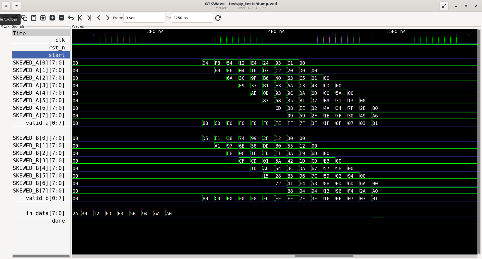
I verified the design at three layers, partly because I was being thorough and partly because I’d been burned earlier by trusting linters. Verilator can give you a clean lint report on RTL that does the wrong thing. For example, I had an FSM that lint-passed but had running <= 1'b0 where it should have been 1'b1. The bug only showed up when I actually ran a simulation and watched the cycle counter never advance. Lint clean isn’t correct. Behaviour tested is correct.
Unit tests, written in SystemVerilog and run under Verilator, cover the leaf modules. The PE testbench includes a 65,536-iteration MAC stress test that walks every possible INT8 × INT8 combination. The skew testbench has six directed tests: pattern correctness, distinguishing real zeros from padding zeros, matrix latching on start, mid-operation reset, signed extremes, and back-to-back operation.
Integration tests are written in Python with cocotb. The harness generates 10,000 random INT8 matrix pairs using a seeded PRNG, runs them through the RTL, and compares the output bit-exactly against a NumPy reference. Both 4×4 and 8×8 configurations pass with zero RTL changes. I just flipped the parameters.
| Configuration | Tests | Wall time | Sim time | Result |
|---|---|---|---|---|
| 4 × 4 | 10,000 | 5.27 s | 1,500,030 ns | PASS |
| 8 × 8 | 10,000 | 13.01 s | 2,700,030 ns | PASS |
Synthesis ran in Vivado 2025.2 against the xc7a100tcsg324-1 part (Nexys A7-100T). The bare array synthesizes in out-of-context mode and closes timing at the 100 MHz constraint with +3.759 ns of slack and zero latches. Sixty-four DSP48E1 slices are used, exactly one per PE, which is what the use_dsp attribute is supposed to do.
What I’d Do Differently
Looking back, the thing that cost me the most time wasn’t the architecture. It was a bug pattern I kept introducing in the testbenches. Whenever I had a block of code that operated on the A matrix and I needed an equivalent block for B, I’d copy the A block and forget to rename one of the references. This happened three times across two different files. The fix, eventually, was to use find-and-replace as the first step after pasting, before doing any other edits, so any leftover A reference would stand out. That’s the kind of discipline you only learn by being burned by it.
The other thing I’d reconsider is the test naming. I had a test called “Real vs Padding Zero” that didn’t actually plant any zeros in the input. It was just another randomized test that happened to live in that block. Tests that don’t exercise their named claim are worse than no tests, because they create false confidence. I rewrote it once I caught the issue, but I should have been more careful when I wrote it the first time.
Up Next
This is the first of seven milestones. M2 is the software side: training a small GPT in PyTorch, doing post-training INT8 quantization, and building a pure-NumPy inference engine that becomes the bit-accurate reference for the hardware verification I’ll do in M3. M3 is where the actually novel piece of the capstone lives. A compute-in-memory attention block where the K/V cache sits in BRAM and dot products are computed by an adder tree wired directly to the read ports.
Project status: M1 complete and verified. Active development continues toward the M2 software pipeline.
Synthesis & timing
| Stage | Frequency | Slack | Area |
|---|---|---|---|
| Implementation (OOC, Vivado 2025.2) | 160 MHz | +3.759 ns | 2,256 LUT · 64 DSP48E1 |
| Implementation with wrapper (full impl) | 117 MHz | +1.450 ns | 2,180 LUT · 64 DSP48E1 |