| Constraint Met | 25 MHz (40 ns) with +22.298 ns worst-case setup slack |
|---|---|
| Worst Hold Slack | +0.330 ns across every PVT corner |
| Power | 11.2 mW total (7.0 mW internal, 4.2 mW switching) at 3.3 V |
| Die Area | 1.23 mm² (1110 × 1110 µm), 32.9% utilization |
| DRC | 0 violations (Magic + KLayout) |
| LVS | Clean — circuits match uniquely |
| IR Drop | 0.01% worst-case (227 µV on 3.3 V VDD) |
Compute-in-memory exists because moving data costs more than computing on it. In a conventional accelerator, weights live in SRAM, get read out onto a bus, and travel to a separate MAC array before any arithmetic happens — and in INT8 inference, that read-and-move step burns more energy than the multiply-accumulate itself. The pitch behind CIM is to skip the move: do the multiply-accumulate inside the memory array, right at the bitcell, so a weight never has to leave the row it’s stored in.
This project is a 32×32 digital CIM macro built for IEEE SSCS’s PICO Chipathon 2026 — a full custom 9T SRAM bitcell, a digital MAC datapath wrapped around it, and a complete RTL-to-GDS flow on the GF180MCU 180 nm open PDK. It’s “digital” CIM rather than analog: the bitcells store bits, not charge-domain analog values, and the multiply-accumulate is done with real AND gates and an adder tree rather than a bitline current sum. That trade gives up some of the density and energy advantage a full analog CIM macro could offer, but in exchange the design verifies like ordinary digital logic — bit-exact, corner-closed, and signoff-clean — instead of needing statistical/Monte Carlo characterization to trust the output.
The Bitcell
The bitcell’s starting point was 6T, and the first real decision was moving off it to an 8T-family cell with a dedicated read port. A plain 6T cell reads and writes through the same pass-gates, which means a read can disturb the stored value if the cell is weakly written. Adding a separate read port decouples the two: read-disturb sweeps at the SS corner (125°C, VDD = 2.97V) confirm the stored node stays flat regardless of how hard the read bit-line is toggled, for both a stored 1 and a stored 0. That’s the core argument for 8T-style cells over 6T in a compute-in-memory context specifically, since every column fires on every cycle — a 6T cell doing that many reads per operation without a decoupled port would be a real disturb risk.
The design went through a full schematic review on an 8T cell — SPICE-characterized for hold SNM (≈0.93V at the 125°C hot corner, via the Seevinck rotated-coordinate method), write margin, and the AND-multiply truth table, on top of the read-disturb sweeps above. That review surfaced an architectural flaw in the 8T cell itself, which forced a second iteration onto the current 9T cell — the one that carried the DRC/LVS signoff and went to layout.
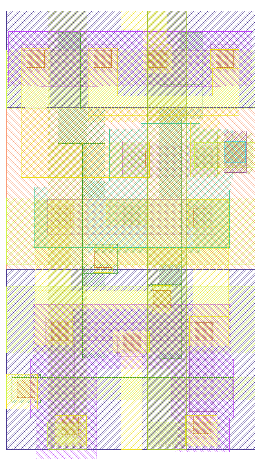
9T_tileable), rendered directly from its GDS — this is the single cell that gets tiled 32×32 to form the array, not the array macro itself. Pinch/scroll to zoom into the layer detail.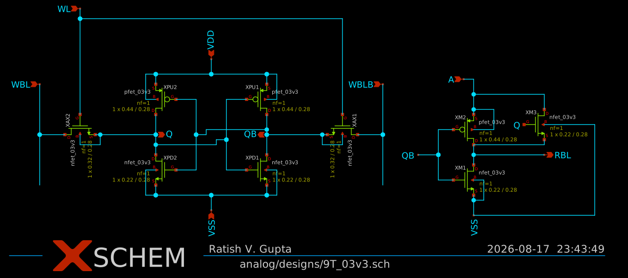
9T_03v3.sch): the standard 6T cross-coupled inverter pair (XPU1/XPU2/XPD1/XPD2 plus access transistors XAX1/XAX2) with a 3-transistor read stack (XM1/XM2/XM3) added for the decoupled RBL read/compute port — the 6T + 3T that makes it “9T.”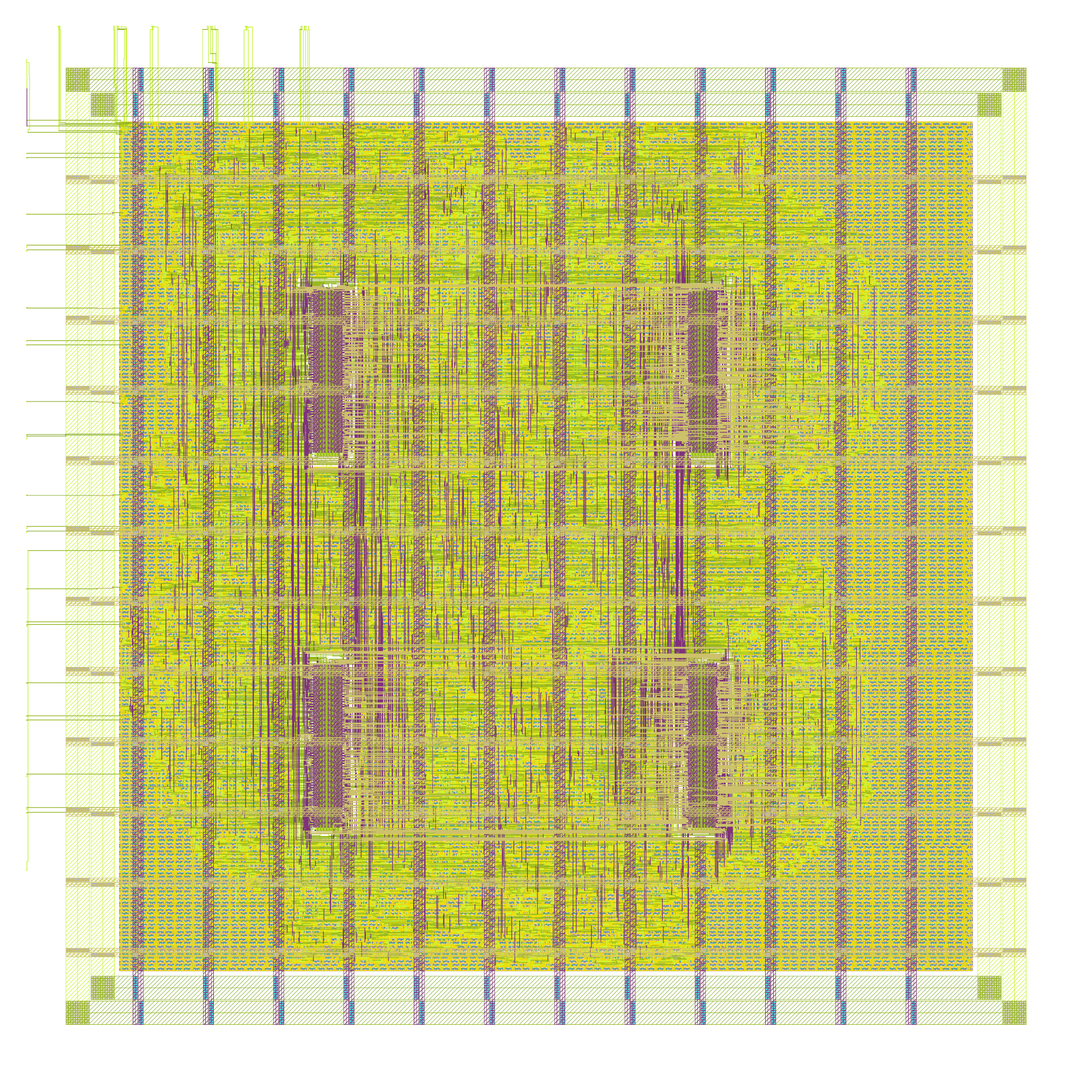
The 9T layout (sram_32x8_9T) is hand-drawn in Magic and carried its own DRC/LVS signoff before being hardened into a macro and dropped into the digital flow as a black box, the same way you’d treat any vendor-hardened SRAM.
Architecture
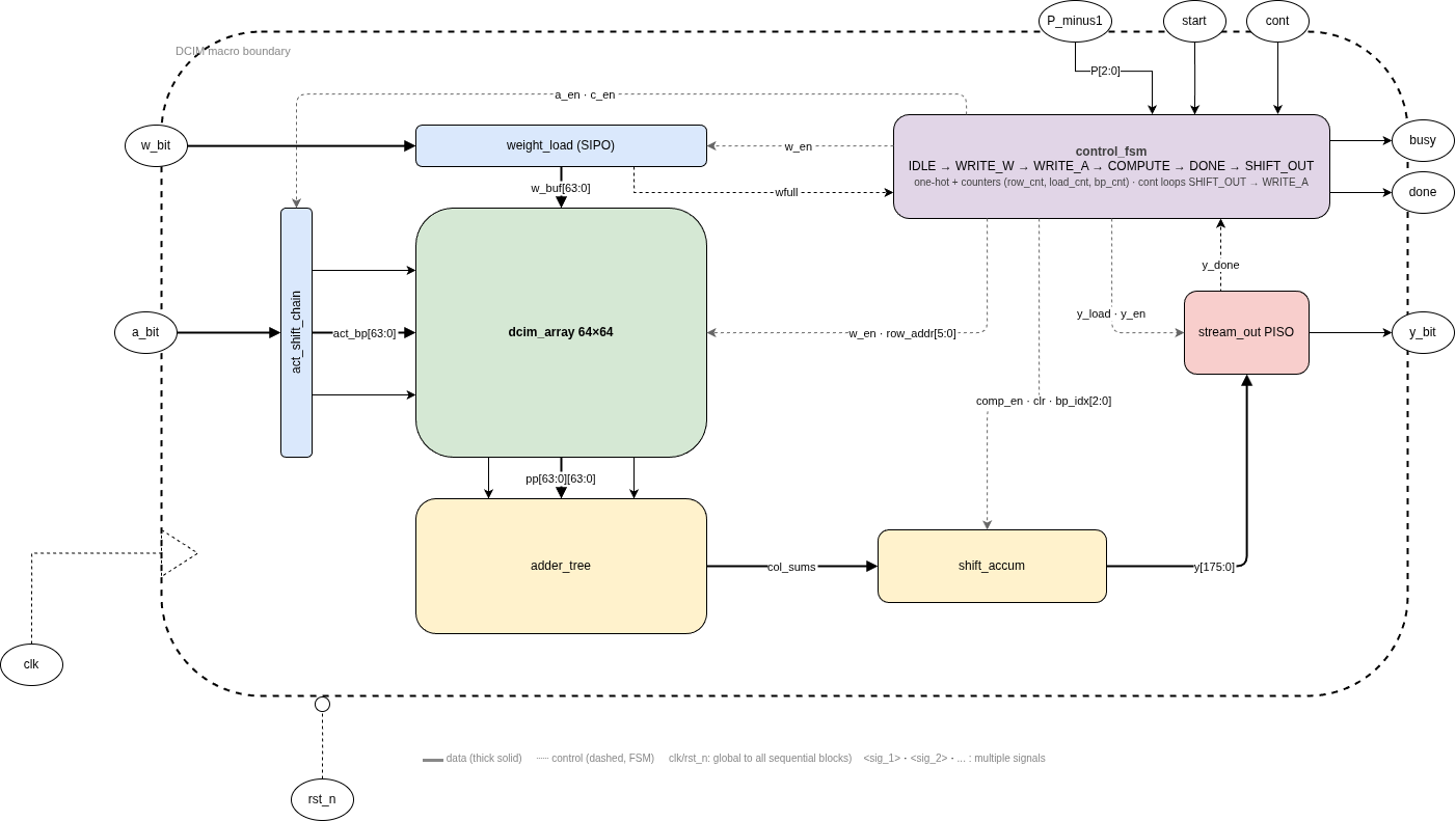
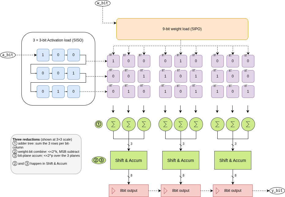
The array is 32 rows × 32 columns (ROWS = 32, COLS = N_WEIGHTS × DW = 4 × 8), holding four INT8 weight vectors side by side. The compute style is bit-serial activations, bit-parallel weights: a full INT8 weight sits resident in its row for the whole computation, while the matching activation is streamed in one bit at a time, least-significant bit-plane first. Each cycle, an AND-multiply matrix ANDs the current activation bit against every stored weight bit in parallel — every cell computes RBL = ~(Q · A) against its own stationary weight bit, so there’s no dedicated multiplier hardware anywhere in the array.
Reconstructing a full INT8 × INT8 dot product out of that one-bit-at-a-time AND array takes three separate reductions, each handled by its own module:
- Vertical (
adder_tree.sv): sums all 32 rows within a bit-column, since a dot product sums across the row dimension. - Horizontal (
col_adder.sv): combines the per-column sums by weight-bit significance — each column’s contribution is left-shifted by its bit position before being added in, with the MSB column subtracted rather than added to handle the signed, two’s-complement weight. - Temporal (
lane_shift_accum.sv/shift_accum.sv): holds a running sum across thePbit-planes of the activation, shifting it left by one bit between planes.
Running P bit-planes — activation precision is runtime-configurable from 1 to 8 bits via P_minus1 — and letting that temporal shift-accumulate stage do its work reconstructs the full product, the same shift-and-add decomposition you’d do in software, just spread across a clock domain instead of an ALU. The output accumulator is 21 bits wide (DW + A_MAX_BITS + $clog2(ROWS) = 8 + 8 + 5), sized to hold a full 32-deep INT8 dot product without overflow.
Controller
A single-bank, one-hot FSM drives the whole datapath:
IDLE → WRITE_W → WRITE_A → COMPUTE → DONE → SHIFT_OUTcase (state)
IDLE: begin
if (start)
next_state = WRITE_W;
end
WRITE_W: begin
// Exit once all 32 weight rows have been assembled and latched
if (row_cnt == unsigned'(RW'(ROWS-1)) && wfull)
next_state = WRITE_A;
end
WRITE_A: begin
// 256 activation bits (DW * ROWS), streamed bit-serial
if (load_cnt == unsigned'(LW'(DW*ROWS-1)))
next_state = COMPUTE;
end
COMPUTE: begin
// Run P bit-planes; P is runtime-configurable via P_minus1
if (bp_cnt == P_minus1)
next_state = DONE;
end
DONE: begin
next_state = SHIFT_OUT;
end
SHIFT_OUT: begin
// cont sampled here, not in DONE — host holds `cont` through the drain
if (y_done) begin
if (cont) next_state = WRITE_A;
else next_state = IDLE;
end
end
default: next_state = IDLE; // one-hot bit error: restart safely
endcase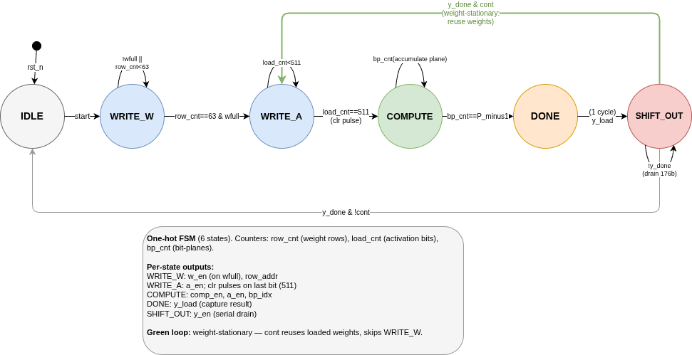
WRITE_W loads the 32 weight rows; row_cnt only advances when the weight front-end has an assembled row ready (wfull), not every cycle, since the incoming weight bits are serialized before they land. WRITE_A streams the DW×ROWS = 256 activation bits and pulses clr on the very last cycle — one cycle before COMPUTE starts, never overlapping it, since clearing on the same cycle as the first bit-plane’s accumulate would silently drop the LSB plane. That ordering is easy to get backwards and hard to catch without a targeted test, which is part of why it’s called out specifically in the verification coverage below.
The FSM also implements weight-stationary reuse: if the host holds cont high through the SHIFT_OUT drain, the next cycle loops straight back to WRITE_A instead of IDLE, skipping WRITE_W entirely. A resident set of weights can run through many activation vectors back-to-back without ever being reloaded — the whole point of doing compute-in-memory in the first place, since the weight only pays its read cost once.
Physical Signoff
The full flow runs through LibreLane on the GF180MCU 0.18 µm PDK, out to Magic + KLayout DRC, LVS, antenna, and multi-corner STA.
| Check | Result |
|---|---|
| DRC (Magic + KLayout) | 0 violations |
| LVS | Clean — circuits match uniquely |
| Antenna | Passed |
| Setup (worst, all corners) | +22.298 ns @ 25 MHz (40 ns) constraint |
| Hold (worst, all corners) | +0.330 ns |
| IR drop (worst-case) | 0.01% (227 µV on 3.3 V VDD) |
| Lint | 0 errors, 0 inferred latches |
Timing was checked across all nine PVT corners LibreLane sweeps by default — nominal/min/max at tt_025C_3v30, ff_n40C_3v60, and ss_125C_3v00 — with zero setup or hold violations and zero TNS anywhere in the sweep. Total power comes to 11.2 mW at 3.3 V (7.0 mW internal, 4.2 mW switching, negligible leakage), and the die sits at 1.23 mm² (1110 × 1110 µm) with 32.9% core utilization. All three signoff categories — DRC, LVS, antenna — come back clean in the manufacturability report, which is the bar for “ready to submit,” not just “simulates correctly.”
Verification
Verification runs on cocotb + Verilator against a bit-exact Python/NumPy golden model that mirrors the hardware’s own decomposition — bit-serial activations, bit-parallel weights, same shift-and-add reconstruction — rather than just checking the final product against a plain NumPy matmul. Every test in the suite runs in both RTL and gate-level mode, the latter against the actual post-synthesis netlist (final/nl/A07_dcim_top.nl.v), so the same coverage exercises both the design intent and what LibreLane actually built.
Coverage includes:
- Full-precision matvec across multiple random seeds (not one fixed draw).
- Reduced-precision sweeps, multiple seeds × multiple values of
P, plus a fixed-seed sweep across the fullP = 1..DWrange specifically to hit theP = 1boundary. - Sign/magnitude edge cases: all-zero, max-positive, max-negative (−128, the asymmetric two’s-complement corner), and alternating min/max patterns.
- Weight-stationary reuse (
cont) across multiple seeds, including varyingPwithin a single continuous run — not just one fixed precision held for the whole reuse loop. - Back-to-back fresh weight loads with no hard reset in between —
start → run → IDLE → start again, loading a completely different weight matrix the second time.
That last case caught a real bug. weight_load.sv’s internal shift counter has no state-based reset — it only clears via the wshift_en enable the FSM drives — and the FSM asserts that enable for one cycle longer than the 1024 shifts actually needed, because the row-count-rollover transition cycle is still counted as WRITE_W. That extra shift permanently offsets the counter’s phase for the next weight load unless something resets it in between. It’s not a testbench artifact; it’s a real property of the signed-off RTL, traced cycle-by-cycle against weight_load.sv and control_fsm.sv before the test was even written. Any host that loads more than one weight matrix per power-up needs this path exercised, which is exactly why it’s a named test rather than something left to be caught incidentally by a random seed.
What’s Next
The chipathon submission is signoff-complete and on track for tapeout through the program. The natural next step is closing the loop between this macro and the systolic-array capstone project — the accumulator width, precision-scaling scheme, and weight-stationary reuse model here were designed with that eventual integration in mind, though the two are independent efforts today, not stages of the same pipeline.
Synthesis & timing
| Stage | Frequency | Slack | Area |
|---|---|---|---|
| Core signoff (dcim_top macro, LibreLane, GF180MCU 0.18 µm) | 25 MHz (40 ns constraint) | +22.298 ns setup / +0.330 ns hold (worst across nom/min/max × tt/ff/ss) | 802,857 µm² instance area · 1.23 mm² die |